




On June 2, 2020, the launching meeting of the special project *Photosensitive Temporary Bonding Materials and Key Equipment for Ultra-Thinning Process of High-end Chips* under the Guangdong Provincial Key Field R&D Program titled "Key Electronic Information Materials" was successfully held at the Bay Area New Technology and Product Exhibition Center in Bao'an District, Shenzhen. The project was led by Shenzhen Samcien New Materials Technology Co., Ltd., in collaboration with Han's Laser Technology Industry Group Co., Ltd., Shenzhen International Innovation Institute for Advanced Electronic Materials and South China University of Technology.
More than 20 attendees were present at the launching meeting, including investigator Zhang Zhitong from the High-tech Division of Guangdong Department of Science and Technology, Party Secretary Chen Zhixiang of Guangdong Productivity Promotion Center, Deputy Director Fu Yuemin from the Materials and Energy Division of Shenzhen Science, Technology and Innovation Commission, Deputy Director Zhang Dai of Bao'an District Science and Technology Innovation Bureau, Director Sun Rong of Shenzhen International Innovation Institute for Advanced Electronic Materials, senior advanced packaging expert Dr. Zhang Li, distinguished expert Professor Xu Jian from Shenzhen University, project leader Researcher Zhang Guoping, as well as principals and team members of all participating institutions.
At the outset, Investigator Zhang Zhitong delivered a speech. He stated that since the launch of the Guangdong Provincial Key Field R&D Program in 2018, the province has been committed to advancing scientific and technological development and breaking bottlenecks in core technologies. He stressed that such key projects must be product-oriented, and all teams should work closely to deliver applicable technological achievements. Next, Deputy Director Fu Yuemin spoke. He expressed gratitude to the Department of Science and Technology of Guangdong Province for its recognition and support for tech enterprises and research institutions in Shenzhen, and noted that the Shenzhen Science, Technology and Innovation Commission would offer supporting policies for the project. Deputy Director Zhang Dai mentioned that three out of the four participating organizations of the project are based in Bao'an District. The Shenzhen International Innovation Institute for Advanced Electronic Materials is also the first new-type research institute introduced by the Bao'an District Government, and the district will offer full support to ensure smooth project implementation. Director Sun Rong said the temporary bonding material technology at the core of the project has undergone eight years of research and development before gaining approval from the provincial science authority. She thanked governments at provincial, municipal and district levels for their strong backing. On behalf of the R&D team, she pledged to keep pursuing innovative research, accelerate the industrialization of research outcomes, and contribute to the development of China's integrated circuit industry.
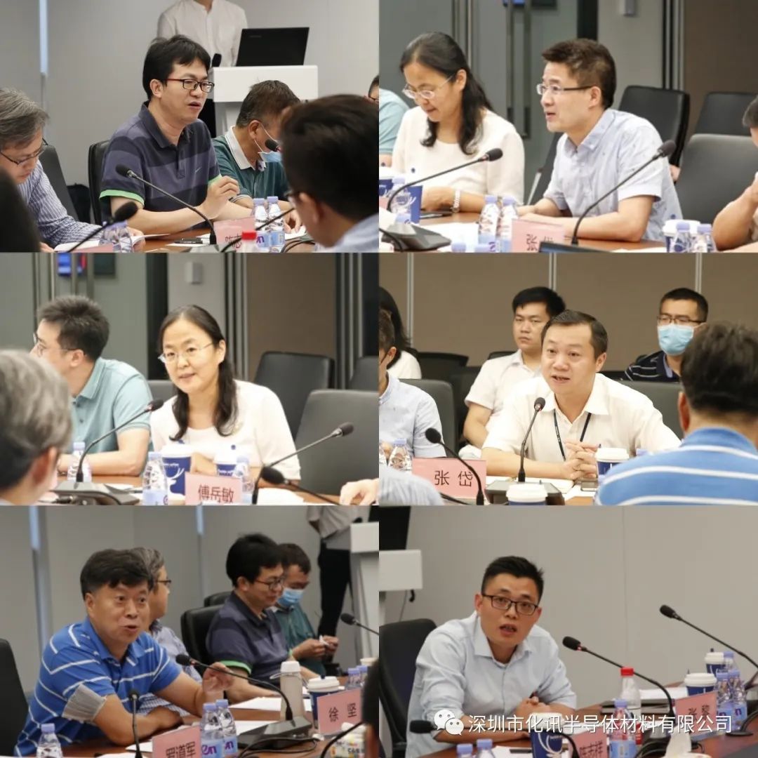
Speeches by Attending Leaders and Experts
Wei Wenqiu, Project Manager of Guangdong Productivity Promotion Center, delivered a report on the management requirements for projects under the Guangdong Provincial Key Field R&D Program on behalf of the competent authority. He interpreted relevant official documents, emphasized the legal liability of the leading entity and the primary responsibility of the project leader. He also required all parties to work out detailed implementation plans, clarify tasks and responsibilities of each participant, improve project management systems and push ahead with project execution.
Afterwards, Researcher Zhang Guoping, the project leader, gave a detailed presentation on the project background, existing technical foundations, implementation schedule and management rules. Xia Jianwen, General Manager of Shenzhen Samcien New Materials Technology Co., Ltd. (the leading company), Wu Lijie, R&D Director of the Display and Semiconductor Equipment Division at Han's Laser, and Professor Liu Lan from South China University of Technology respectively reported on the sub-projects undertaken by their respective organizations.
In the project implementation plan review session, specially invited expert Dr. Zhang Li emphasized that the temporary bonding material technology targeted by this project boasts broad application prospects in third-generation semiconductors, 3D memory chip packaging, and 2.5D/3D packaging fields. He suggested strengthening team building, prioritizing talent investment, and sustaining technological innovation throughout project implementation. Professor Xu Jian recommended adopting multiple final evaluation methods including random inspections, customer certification and result-oriented assessment for project management. He urged the project team to maintain a sense of urgency, accelerate R&D progress, and contribute sooner to the independent, controllable development of China’s integrated circuit industry. Chen Zhitao, Dean of Guangdong Semiconductor Industry Research Institute, expected that breakthroughs in temporary bonding technology could drive the development of related new technologies and achieve comprehensive industrial progress. Luo Daojun, Director of the China Electronic Product Reliability and Environmental Testing Research Institute, stressed the importance of failure analysis in the R&D of materials and equipment. He also reminded the team to focus on research details, as well as material storage and shelf-life management.
The participating leaders and experts held in-depth discussions on the implementation plan proposed by the project team and put forward valuable suggestions to facilitate the smooth progress of the project.
Finally, Investigator Zhang Zhitong concluded that the project's innovative R&D model combining materials and equipment will surely deliver practically valuable research outcomes. He expressed full confidence in the smooth execution of the project, and encouraged all participating organizations to communicate and cooperate closely so as to apply the R&D achievements to China's integrated circuit industry at an early date. Pictures
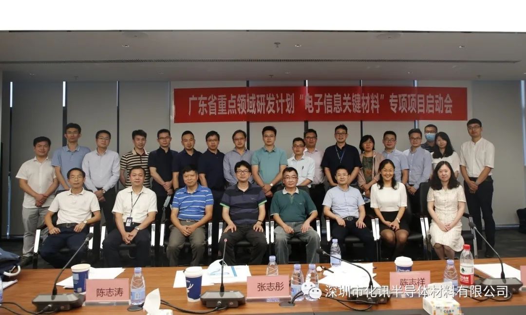
Group Photo of Participants